Advanced Micro Devices AI chips: The evolution of Instinct
AMD’s Instinct MI250X shipped with 128 GB of HBM2e and 3.2 TB/s of peak memory bandwidth in late 2021.
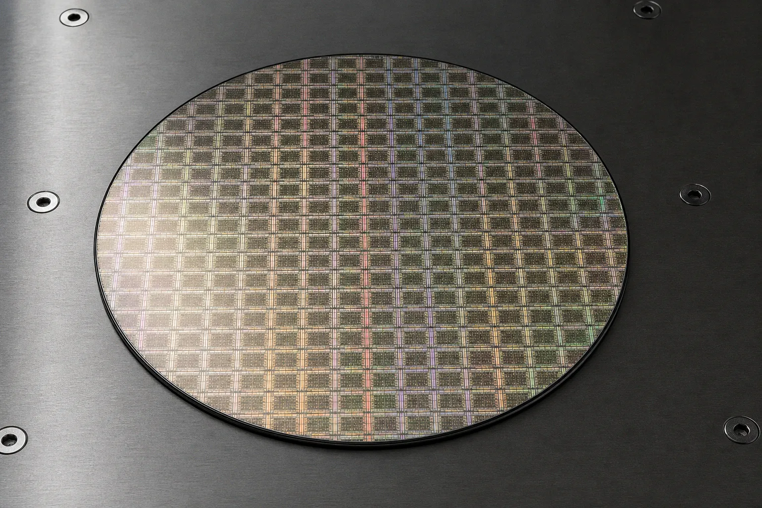
The MI355X platform announced less than four years later places 2.3 TB of HBM3E beside eight accelerators and quotes 80.5 PFLOPs of peak MXFP4 matrix performance. The forward-looking Helios reference design then extends the unit of competition again: 72 GPUs, 31 TB of HBM4, liquid cooling, 260 TB/s of aggregate scale-up bandwidth.
That progression is more consequential than a sequence of larger FLOPs figures. The evolution of advanced micro devices AI chips has been a shift from accelerators designed principally for exascale HPC installations toward systems designed around the practical bottlenecks of frontier-model inference and training: parameter count, memory capacity, memory bandwidth, interconnect topology, rack power density, and the software path required to make thousands of devices behave as one cluster.
AMD is still operating in a market where the incumbent CUDA ecosystem establishes the baseline against which every alternative is measured. But the Instinct roadmap is no longer merely a component-level response. MI300X made HBM capacity the central argument; MI325X increased that capacity without changing the underlying CDNA 3 compute-unit count; MI355X introduced a new low-precision arithmetic regime; Helios makes the rack, cooling manifold, NIC and fabric part of the accelerator proposition.
From exascale HPC to AI density: the CDNA trajectory
The MI250X, launched on November 8, 2021, was a distinctly HPC-shaped product. Built on CDNA 2, it provided 220 compute units, 128 GB of HBM2e, and 3.2 TB/s peak memory bandwidth. Its peak TDP was specified in 500 W and 560 W configurations. Those numbers were substantial for the period, but the product’s framing reflected an era in which double-precision throughput, large-scale simulation, and tightly coupled supercomputing workloads remained central to accelerator design.
The later Instinct products did not abandon that lineage. They changed which resource was treated as scarce.
For modern transformer workloads, a device’s useful throughput is constrained by more than matrix-unit peak. Model weights, activations, key-value caches, optimizer state, and communication buffers must all reside somewhere. If they do not fit in local high-bandwidth memory, the system begins paying for transfers across slower tiers or fragmenting a model across more devices. That increases collective-communication pressure and can raise end-to-end latency even when nominal compute capacity remains available.
The MI300X, launched on December 6, 2023, was therefore an architectural pivot. CDNA 3 increased the accelerator to 304 compute units and paired them with 192 GB of HBM3 at 5.3 TB/s peak bandwidth. AMD listed 2.61 PFLOPs of peak FP8 performance and 750 W peak typical board power. The key commercial number, however, was frequently the 192 GB memory figure rather than the FP8 headline.
An eight-GPU MI300X Universal Baseboard 2.0 contains 1.5 TB of HBM3. That matters because an eight-way baseboard is the actual local unit from which a great deal of AI infrastructure is assembled. It is not one monolithic GPU; it is an OCP-based platform containing eight OAM modules. But for model placement, tensor parallelism, and the operational arithmetic of serving large parameter counts, the aggregate memory envelope is the relevant starting point.
In large-model systems, HBM capacity is not a peripheral specification. It determines how much parallelism must be purchased before computation even begins.
The distinction between capacity and bandwidth should be kept explicit. Capacity determines whether weights and working state can be retained locally. Bandwidth determines how quickly those bytes can be supplied to matrix engines. A bandwidth-rich accelerator can still be awkward for a model whose quantized or unquantized weight footprint does not fit efficiently; a large-memory accelerator can still underperform on bandwidth-bound decoding or communication-heavy distributed training. The Instinct line has been moving both variables upward, rather than presenting compute as a standalone metric.
MI300X and MI325X: a memory-first iteration
The MI325X, released on October 10, 2024, did not represent a wholesale architecture replacement. It retained the CDNA 3 design and the same 304 compute units as the MI300X. Its principal change was memory: 256 GB of HBM3E per accelerator, with 6 TB/s peak memory bandwidth and 1,000 W peak typical board power.
That is an unusually direct statement of product intent. Rather than recasting the chip around a new compute-unit topology, AMD enlarged the HBM pool and increased the rate at which it could be accessed. An eight-GPU MI325X platform consequently exposes 2.048 TB of HBM3E. It also specifies 896 GB/s aggregate bidirectional peer-to-peer I/O bandwidth.
The generational comparison is clearer when the specifications are placed beside each other, while avoiding the common error of treating every column as a direct application-performance result.
| Parameter | Instinct MI250X | Instinct MI300X | Instinct MI325X |
|---|---|---|---|
| Architecture | CDNA 2 | CDNA 3 | CDNA 3 |
| Launch date | November 2021 | December 2023 | October 2024 |
| Compute units | 220 | 304 | 304 |
| HBM capacity per GPU | 128 GB HBM2e | 192 GB HBM3 | 256 GB HBM3E |
| Peak memory bandwidth | 3.2 TB/s | 5.3 TB/s | 6 TB/s |
| Peak typical board power | 500 W or 560 W configuration | 750 W | 1,000 W |
| Reported low-precision peak | — | 2.61 PFLOPs FP8 | Datatype-dependent figures |
The MI325X is sometimes still described as a 288 GB part. That description originates from AMD’s June 2024 roadmap projection, not from the final product. The launch materials and product specifications list 256 GB of HBM3E. For infrastructure planning, this is not a pedantic correction: a 32 GB discrepancy per GPU becomes 256 GB across an eight-way node and expands further at cluster scale.
The higher board-power figure is equally material. It means a memory-capacity improvement cannot be separated from rack engineering. A cluster buyer is not selecting only a GPU SKU; they are selecting the electrical distribution, cooling approach, mechanical density, serviceability model, and network architecture that allow the SKU to operate near its intended envelope.
This is where the comparison with prior GPU generations becomes less tidy. The MI250X existed comfortably in a world where accelerator power was already difficult but more often handled through familiar server designs. MI325X-class hardware pushes the deployment discussion toward liquid cooling and rack-level thermal design. The compute device is becoming less separable from its physical substrate.
The software layer is similarly inseparable. The ROCm open software ecosystem is AMD’s mechanism for exposing kernels, compilers, communication libraries, and framework integrations to AI workloads. Its strategic relevance is straightforward: a larger HBM pool cannot compensate for an incomplete operator path, fragile distributed runtime, or poor kernel efficiency at the quantization formats actually used in production. Yet software maturity cannot be inferred from any one accelerator specification sheet. It must be evaluated with a particular model, precision policy, framework version, batch profile, and cluster topology.
MI355X and the MXFP4 arithmetic shift
AMD’s MI355X platform, launched on June 12, 2025, moved the Instinct family to fourth-generation CDNA. The platform consists of eight MI355X OAM GPUs, with 2.3 TB of HBM3E in aggregate and 8 TB/s of memory bandwidth per OAM. AMD rates the full platform at 80.5 PFLOPs of peak MXFP4 matrix performance.
The important term in that figure is MXFP4, not simply 80.5 PFLOPs.
Low-precision formats have become central because model execution is increasingly shaped by the ratio between useful arithmetic and bytes moved through memory. A four-bit representation can reduce weight storage and bandwidth demand relative to higher-precision formats, but quantization is not a free scalar reduction. Accuracy retention depends on the model architecture, calibration method, per-block scaling behavior, outlier handling, operator support, and whether the model is being trained, fine-tuned, prefilling prompts, or decoding tokens one at a time.
AMD reports MI350-series performance across MXFP4, MXFP6, MXFP8, and OCP-FP8. Those categories should not be collapsed into a single generic “AI performance” number. Peak theoretical matrix throughput changes with datatype, structured sparsity assumptions where applicable, and measurement scope. An eight-GPU platform figure cannot be equated automatically with a single-GPU result; nor can peak FLOPs be translated directly into tokens per second, training duration, energy per token, or cloud cost.
A useful reading of the MI355X is therefore not that it provides a universally measurable multiple of prior Instinct performance. It is that AMD has shifted the architecture toward the precision formats that increasingly govern inference economics. At frontier-model scale, especially for memory-resident serving, the question is not whether a chip supports low precision in the abstract. It is whether the compiler, kernels, collective operations, and serving stack sustain that precision without inserting bottlenecks elsewhere.
Three constraints determine whether the MXFP4 era materially changes deployment economics:
1. Model-level numerical tolerance. A model that remains stable under a given quantization scheme can reduce memory traffic and expand the practical parameter count per node. A model requiring fallback operations or higher-precision outlier paths will realize a different gain.
2. Memory and fabric balance. Eight TB/s per OAM is significant, but inference throughput can remain limited by cross-device transfers when tensor parallelism is required. Reducing bits per weight helps, yet it does not eliminate synchronization or key-value-cache movement.
3. Software-path completeness. The theoretical data format must be supported across the relevant runtime: attention kernels, GEMMs, mixture-of-experts routing, collective communication, graph compilation, and production observability. Unsupported corners are where peak arithmetic turns back into latency.
FLOPs describe available arithmetic; deployment performance is determined by the slowest movement of parameters, activations, cache state, and collective traffic around that arithmetic.
The AMD AI hardware roadmap is consequently becoming a roadmap for numerical formats and system balance, not just transistor density. That is a more difficult proposition to benchmark, but it is closer to how operators make purchase decisions.
Helios turns the rack into the product
Helios is AMD’s clearest acknowledgment that a discrete accelerator is no longer the complete product boundary. It is a reference design, not a retail AMD server, and it integrates 72 CDNA 5-based MI455X GPUs with EPYC “Venice” CPUs, Pensando “Vulcano” AI NICs, OCP Open Rack Wide, UALink, and Ultra Ethernet Consortium standards.
The stated specifications are rack-scale: 31 TB of HBM4 across 72 MI455X GPUs, up to 432 GB of HBM4 per GPU, 19.6 TB/s of memory bandwidth per GPU, 260 TB/s aggregate scale-up bandwidth, and 43 TB/s scale-out bandwidth.
The magnitude of the local memory pool is the obvious headline. But the more structural change lies in how Helios divides communication.
Scale-up bandwidth concerns the high-bandwidth domain used to bind accelerators closely enough for a large model or training job to be partitioned across them. Scale-out bandwidth concerns the network domain used to connect larger groups of systems. These are separate engineering problems. A cluster can have excellent network reach and still underperform if the local accelerator domain is constrained; conversely, an exceptionally dense rack does not resolve data-parallel all-reduce, storage ingest, control-plane coordination, or cross-rack routing.
UALink is relevant in this context because it addresses the scale-up layer as an open interconnect direction, while Ethernet-based scale-out aligns the design with an infrastructure base that operators already understand and deploy at large scale. The promise is architectural flexibility, not the elimination of topology. The burden shifts to OEMs, cloud operators, and customers to establish the resulting latency, congestion behavior, routing policy, and failure domain in real deployments.
Liquid cooling is also built into the reference design rather than treated as a later facility adaptation. Helios uses a cooling manifold distributing liquid coolant through quick-disconnect connections. That detail is operationally significant. At this density, cooling influences maintenance windows, leak-detection procedures, row-level plumbing, redundancy design, and the degree to which a rack can be serviced without disrupting adjacent systems.
The broader digital infrastructure market is already being shaped by that convergence of compute, power, thermal engineering and networking, a pattern visible across coverage of the digital business and IT industry. In AI clusters, the interaction is particularly severe because utilization targets are high and power excursions are not an incidental condition; they are inherent to the workload.
Helios should therefore be read as a reference architecture intended for OEM and ODM partners, not as proof of a universally available 72-GPU configuration with standardized pricing or identical implementation. The public description does not establish final OEM configurations, availability schedules, or end-customer total cost of ownership. Those variables will depend on the server vendor, fabric choice, facility design, and software qualification path.
The Meta deployment plan and what it actually signals
On May 5, 2026, AMD said that Meta and AMD had announced plans for deployments of up to 6 GW of AMD Instinct GPUs. The first planned 1 GW was described as using a custom MI450-based GPU.
The language matters. This was a deployment plan, not evidence that the entire 6 GW had already been installed and made operational. In a market prone to converting announcements into completed capacity, the distinction is material.
Even as a plan, however, the number indicates the changed scale at which accelerator vendors are being evaluated. Gigawatt-scale commitments are not simply purchase orders for chips. They imply long lead-time coordination across silicon supply, advanced packaging, HBM availability, board manufacturing, power distribution, cooling, buildings, network equipment, and software deployment. A custom MI450-based device further indicates that hyperscale buyers are seeking architectural influence over the hardware deployed at their own fleet scale.
For AMD, the strategic significance is less about one announcement than about the evidence it provides for the company’s direction of travel. The Instinct family began with a strong position in scientific computing and grew into a product sequence increasingly optimized around the memory footprints and quantized arithmetic of large AI models. The next contest is at rack and campus scale, where buyers will assess not only per-GPU capability but the deliverability of a complete, supportable system.
What the Instinct evolution changes for developers and operators
The technical through-line from MI250X to Helios is clear: HBM capacity expanded from 128 GB to a planned 432 GB per MI455X; per-accelerator peak memory bandwidth rose from 3.2 TB/s to a stated 19.6 TB/s in Helios; the deployment unit expanded from an accelerator and an eight-GPU baseboard to an explicitly specified 72-GPU rack-scale design.
That progression changes the questions developers should ask of infrastructure. The first question is no longer only which accelerator has the largest advertised peak. It is whether the intended model fits at the chosen quantization, how much tensor parallelism is required, what communication pattern follows, and where latency accumulates across the serving path. For training, the equivalent calculation includes optimizer-state placement, checkpoint traffic, collective synchronization, and the relationship between local HBM bandwidth and the network fabric.
For operators, the unit of analysis has moved from board power to rack thermals, from PCIe enumeration to fabric topology, and from a compiler benchmark to the durability of the complete runtime stack. AMD’s design language increasingly reflects that reality.
The advanced micro devices AI chips story is therefore not a simple succession of faster devices. It is the construction of a competing system architecture around memory density, low-precision execution, open interconnects, Ethernet scale-out, and liquid-cooled rack integration. The final comparison will not be settled by a peak PFLOPs table. It will be settled where these systems are always settled: in sustained utilization, reproducible latency, software reliability, and the ability to deploy capacity faster than the models consume it.